Be ready at the right moment


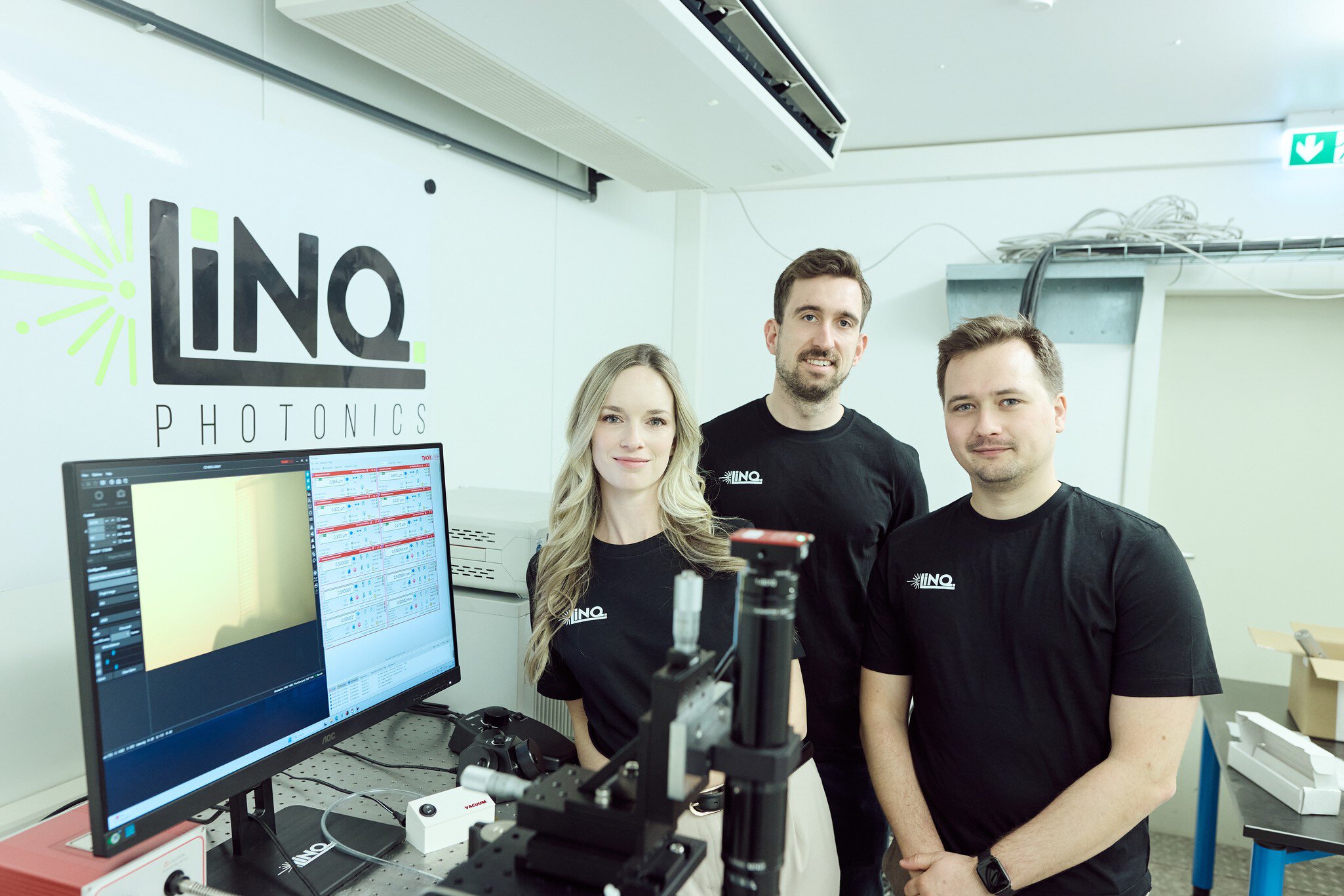
Linq Photonics develops photonic chips for light modulation that improve the performance and scalability of quantum computers. The startup has its origins in the Neuromorphic Quantum Photonics Group at Heidelberg University. Its director, Prof. Wolfram Pernice, serves as a mentor to the team and brings experience from the successful founding of Pixel Photonics and Salience Labs. In this interview, COO Jade Robinson and CTO Julius Römer discuss Linq’s technological approach, the prospects for scaling, and the significance of the World of Quantum for a quantum technology startup.
Mr. Römer and Ms. Robinson, would you like to briefly introduce Linq Photonics to us?
Julius Römer: Sure! We’re a young startup that spun off from Heidelberg University. Our roots lie in Prof. Wolfram Pernice’s Neuromorphic Quantum Photonics Group, where we worked on development projects with quantum computing companies in Munich, among other things. That’s where our current CEO, Rasmus Bankwitz, came up with the idea for a photonic chip that can be used to control quantum computers, particularly those based on atomic and ion traps. That’s because they require precise light pulses at specific wavelengths. In principle, it is the light modulated on our chip that brings the qubits into the correct state for computational operations. Our project partner likes the approach so much that he wants to commercialize it. Based on this feedback, we initiated the startup. Prof. Pernice has already launched two very successful startup projects with Pixel Photonics and Salience Labs and supports our project with advice and practical assistance. We are currently funded through the EXIST Research Transfer program of the Federal Ministry for Economic Affairs and Energy (BMWE). While Rasmus and I are more the tech nerds, Jade brings the necessary business experience to the table.
Jade Robinson: We met at a matchmaking event as part of the XPLORE program at the Technical University of Munich. The program is specifically aimed at teams in the incubation phase. In addition to helping with team building, it offers teams support in defining their business model, target market, and strategic direction. At the time of World of Quantum 2025, we hadn’t yet been officially founded as a GmbH, but we used the platform to present ourselves and our technology to an international audience of experts. The official founding didn’t take place until March 2026.
So you’re just taking your first steps as an entrepreneur. What’s the story behind your photonic chips, and how are they constructed?
Römer: Essentially, it involves light modulation directly on a photonic integrated chip. Our customers need solutions to individually control and manipulate thousands of atoms or ions in quantum computers. This requires specific wavelengths and pulses for which there is no off-the-shelf, cost-effective hardware like the silicon-based components manufactured in high volumes for telecommunications applications.
Our chips are built on a passive platform made of silicon nitride and lithium niobate (LiNbO3) for the active circuits. We have built up the necessary expertise to process these materials and implement modulation in the visible wavelength range from 400 to 1700 nm. This enables us to design chips to meet our customers’ high requirements, optimize them through simulations, and manufacture them. In quantum computing applications, the correct on-to-off ratio is particularly critical. Here, we achieve an extinction ratio of up to 60 dB. Combined with precise phase and amplitude control, this is a unique selling point. Among other things, we integrate beam splitters, optical filters, and multiplexing capabilities onto the chips to bundle different optical signals into a single fiber.
Is it primarily about materials expertise or chip design?
Römer: It’s a mix of both: To build our chip designs, which are optimized in simulations, we need an understanding of materials, packaging expertise, and the ability to control the entire system electronically. We source wafers from specialized suppliers onto which crystalline LiNbO3layers have been deposited using thin-film deposition, and we then integrate the corresponding chip structures, metals, waveguides, and beam splitters into them.
For a newly founded university spin-off, that represents a high degree of vertical integration...
Römer: …we have a fairly large team here at the university and a lot of technical support from experts. And we only implement chips for specific applications, which we first simulate from the ground up. In doing so, we naturally take into account which machines we have access to. We test material formulations and integration concepts. It’s an iterative process in which we can access the university’s infrastructure through the EXIST research transfer program for product development. This is incredibly important because this technical infrastructure is far too expensive for us to purchase at this stage. The purpose of such research transfer programs is for young companies to transfer newly acquired scientific findings directly to the market. Looking ahead, our goal is, of course, to gradually transition away from the university ecosystem and have our chips manufactured in higher volumes at foundries.
Scaling up requires demand from manufacturers of neutral-atom or ion-based quantum computers. Do you expect production volumes to increase that soon?
Robinson: We have several key players among quantum computer manufacturers who are very interested in our chips and have signaled a high demand for our chip technology. They would like to test them in their own systems. Of course, the volume isn’t yet where we’d like it to be.
Römer: There aren’t that many companies manufacturing such quantum computers yet. And before they order chips from us, they naturally want to test them thoroughly first. There are also players in the U.S. pursuing in-house approaches with integrated photonics that are roughly similar to ours. But we’re hearing from the neutral-atom and ion-trap community that they’re looking for a solution like the one we’re developing. It may still take a few years before scaling begins. Until then, we still have a lot of work to do so that we’re ready at the right moment—and can set the standard with our solutions.
The die has not yet been cast regarding which quantum computing platform will prevail. Does your business model account for this uncertainty?
Römer: For now, our plans do not call for rapidly achieving high sales figures. Rather than quantity, our focus is currently on quality and on scaling the quantum systems themselves. Manufacturers face the challenge of scaling computing platforms from 100 to 1,000 or even 10,000 neutral atoms. We see this scaling as an opportunity! Our chips—and our startup—can grow along with them. That’s why the focus right now is less on sheer volume and more on approaches to make our chips ready for rapidly growing demands—from increasingly compact packaging to the ability to control a large number of atoms with precisely timed light pulses. Ultimately, 10,000 atoms will require 10,000 modulators. That is the scaling challenge we aim to solve. The complexity of our chips will increase dramatically. They must do more and more in less and less space. Electronic control, cooling, multiplexing to avoid having to connect 10,000 optical fibers, the arrangement of waveguides, filters, and modulators, as well as reliability, stability, and bandwidth: We want to solve all of this before the market takes off. That’s why we’re expanding our teams in software development and fabrication.
What role does a trade show like World of Quantum play for your young startup?
Robinson: It’s very important. The three of us were there and found key players in our specific ecosystem—both potential customers and suppliers. We held many discussions and made important contacts. It was helpful to be able to reach out to exhibitors from all three “ ” trade shows—World of Quantum, Laser World of Photonics, and automatica—in advance via the web platform at and schedule meetings. Many were open-minded, showed interest in our technology, and had productive discussions with us. Especially on the supplier side—whether foundries, manufacturers of fiber arrays, electronics, ASICs, or FPGAs—there is much new to discover. This applies not only to World of Quantum but to the entire Laser World of Photonics. The coexistence of both trade shows is exactly what we and the entire quantum community need. Among other things, we established a very important contact with a supplier from the UK whose approach aligns perfectly with our own in terms of chip integration and packaging. We hadn’t even heard of the company before. This contact could become very important in terms of scaling up and establishing our manufacturing operations. From that perspective, it was a very good decision for us to be there even before the company was officially founded.